 3 hours ago
2
3 hours ago
2
Tom's Hardware Premium Roadmaps
SK hynix, the world's biggest supplier of high-bandwidth memory (HBM), this week approved a ₩19 trillion ($12.896 billion) investment to build P&T7, a new advanced packaging and test facility in South Korea, dedicated solely to HBM. The plant will likely be the biggest HBM assembly and test facility in the world, but it will almost certainly not be the last HBM packaging and test facility of the same scale and cost going forward, considering the booming demand for memory, which has caused DRAM pricing to skyrocket.
A massive facility
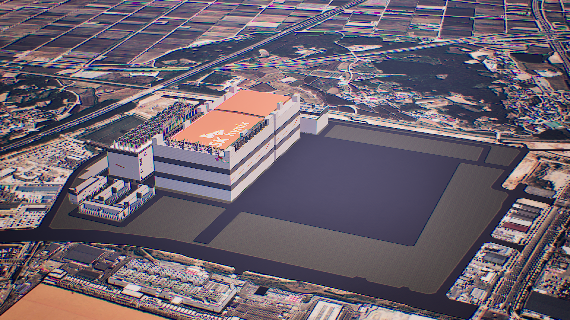
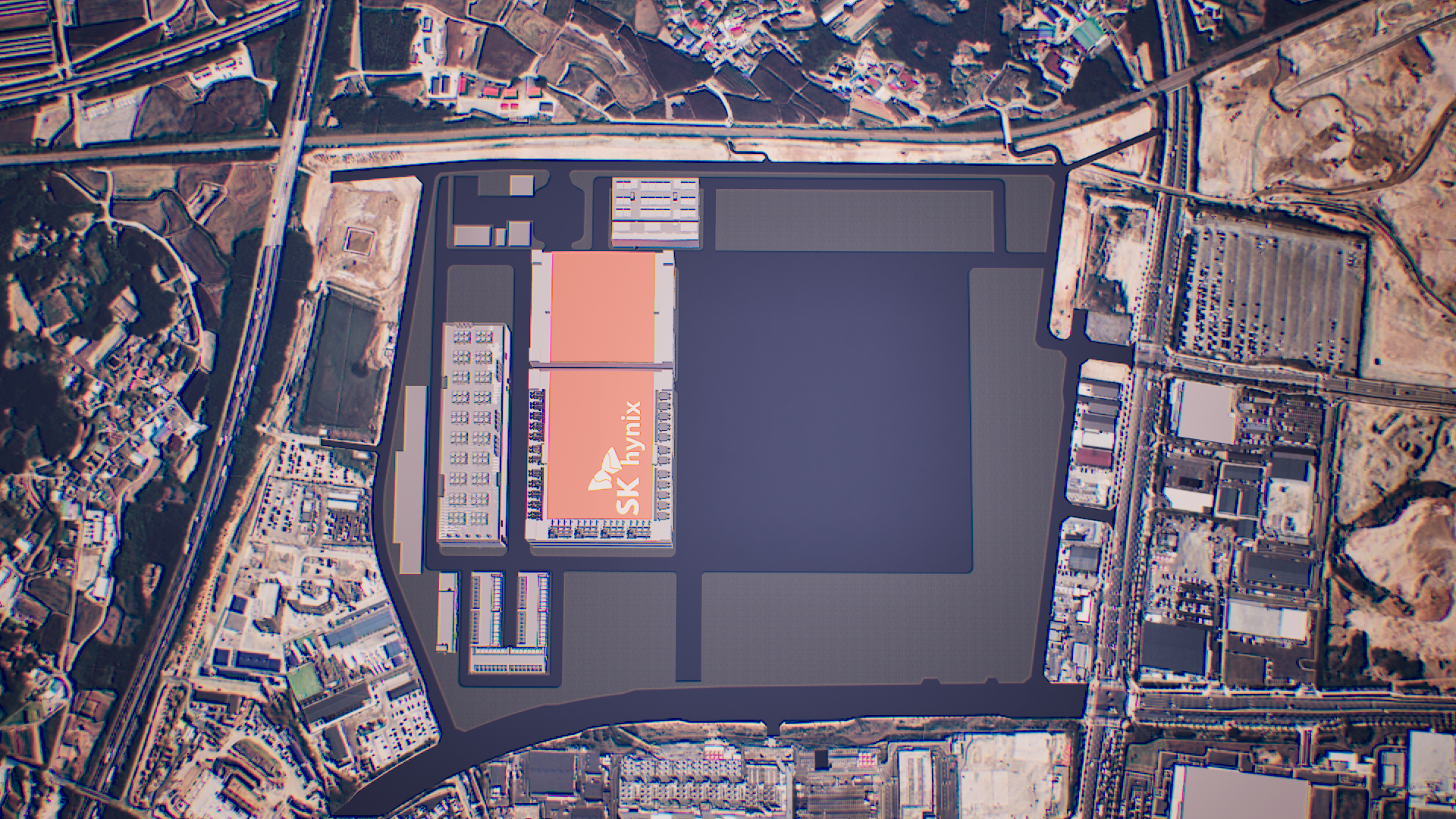
The company plans to construct what it calls P&T7 (Packaging & Testing 7) facility at the Cheongju Technopolis Industrial Complex, on a site measuring approximately 70,000 pyeong (approx. 231,405 square meters or 2,490,822 square feet). Construction is scheduled to begin in April 2026, and completion is targeted for the end of 2027, which is when the building will be finished, and is when SK hynix will begin installing equipment. Due to the equipping phase, expect the plant to come online toward the end of the decade on time for HBM4E, HBM5, and HBM5E types of memory.
The facility's dimensions are massive, resulting in a campus-scale site, rather than a back-end factory plot. For packaging and testing, the Fab P&T7 plot is unusually large; this may reflect the importance of HBM (and other exotic types of memory) assembly for the AI industry specifically, and the memory industry as a whole.
To put the scale into context, Intel's Ocotillo Campus near Chandler, Arizona, spans over 362,727 square meters, but it houses multiple front-end fab buildings, such as Fab 12, Fab 22, Fab 32, Fab 52, and Fab 62. Both Fab 52 and Fab 62 are expected to be capable of processing up to 40,000 wafer starts per month each when fully ramped, which makes them bigger than typical logic fabs run by TSMC.
While HBM packaging is a back-end activity, it still requires complex techniques like etching, lithography, hybrid bonding, and many other steps and tools used in logic production. This explains why HBM testing and packaging facilities are larger than typical back-end facilities.
Nonetheless, HBM packaging is inherently simpler than producing logic, so the scale of SK hynix's P&T7 plant is enormous, even by HBM standards. Its dimensions and investments dwarf SK hynix's HBM testing and assembly plant in West Lafayette, Indiana, which will cost the memory maker $4 billion and will span 39,948 square meters. Yet, keeping in mind that SK hynix expects the compound annual growth rate (CAGR) of HBM to be 33% from 2025 to 2030, it needs all the front-end DRAM and back-end packaging facilities it can build.
A strategic location
A key element of the project is its operational linkage with Fab M15X, a major SK hynix semiconductor manufacturing facility currently located in Cheongju that is currently being equipped with fab tools. The company expects the combined operation of M15X and P&T7 to create a tightly coupled manufacturing ecosystem capable of building HBM dies (which are three to four times larger than commodity DDR5). Therefore, SK hynix can test and package HBM in close proximity, essentially creating a vertically integrated manufacturing facility for HBM or other exotic types of memory that use multi-chip packaging.
The adjacency of Fab M15X and P&T7 is intended to elevate Cheongju into a new core base for SK hynix's AI memory operations, which will optimize production and packaging and can potentially enable the company to respond to market demand for HBM faster than it can today.
As a bonus, the close proximity of the front-end memory fab and the advanced packaging and testing facility will shorten feedback loops between engineers at both facilities, which might positively affect yields and/or performance. In fact, as the industry transits to more sophisticated types of memory for AI accelerators — such as HBM4 with a 2,048-bit interface — the bigger and more sophisticated assembly and testing plants for high-bandwidth memory located close to front-end DRAM fabs make sense.
From a strategic planning perspective, SK hynix says it had evaluated multiple domestic and international locations before selecting Cheongju for P&T7. The decision reflects multiple objectives. Firstly, the vast majority of SK hynix's memory is produced in South Korea, so it is reasonable to build its most advanced testing and packaging facility for AI DRAM nearby. Secondly, P&T7 working in proximity with M15X will reinforce the overall competitiveness of South Korea's semiconductor industry. Thirdly, a large project also supports regional development, a policy promoted by the government.
SK hynix notes that the site selection decision was not purely cost-driven; the company evaluated proximity to existing fabs, infrastructure readiness, and long-term supply-chain resilience. Cheongju was ultimately chosen as the location that balanced industrial efficiency best.
Although SK hynix never mentions it, there is one more factor that likely affected its decision to build its biggest HBM packaging facility in South Korea. Because the vast majority of AI accelerators are made in the region, not only in South Korea, but in Taiwan by TSMC.
Since SK hynix and TSMC share a lot of customers, the two companies work closely with one another. However, due to geopolitical and regional competitive reasons, SK hynix isn't likely to build a major facility in Taiwan, making South Korea the next-best option.
Technological importance
Building an extremely big HBM testing and packaging facility is important for SK hynix, not only from strategic and logistical points of view, but also from a technology development point of view.
Advanced packaging is as critical to HBM as the DRAM front-end fab because of HBM's inherent characteristics — extreme bandwidth, power efficiency, and density. These elements are enabled by the DRAM itself and packaging technology. A single DRAM die does not expose a 1,024-bit or 2,048-bit interface: it's enabled by stacking 8 – 16 dies, each featuring a 128-bit I/O, interconnected with Through Silicon Vias (TSVs), and routed through base dies and Redistribution layers (RDLs). To make everything work properly and according to specification, packaging must ensure bonding accuracy, optimal TSV resistance, and RDL integrity.
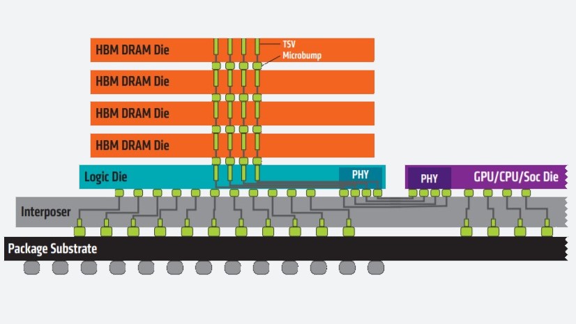
Power efficiency and thermals are also largely determined by packaging, as they define things like TSV and RDL parasitics, micro-bump or hybrid-bond quality, and interposer losses. Some packaging technologies have increased I/O voltage requirements and higher switching losses, which force manufacturers to reduce data transfer rates compared to offerings from their rivals.
Heat-extraction is also a big deal, and it entirely depends on packaging process technology (underfill and mold materials, as well as package-level thermal paths), as the better heat dissipation is between memory dies, the easier it is to cool the whole stack. SK hynix leads the industry with its mass reflow-molded underfill (MR-MUF).
Yield economics also increase the importance of packaging technology: even if a front-end DRAM fab achieves a 99% good die yield, if yield loss during packaging is significant (due to TSV defects, bond misalignment, and/or RDL defects), it hits margins across both the expensive DRAM fab and relatively inexpensive back-end packaging facility. Reliability qualification — burn-in, thermal cycling, and long-duration stress testing — is also performed at the package level and cannot be handled by generic back-end lines.
As HBM scales toward more dies per stack, wider interfaces, tighter pitches, and hybrid bonding, packaging complexity and costs of packaging and testing facilities will rise to logic-fab-class levels, which is probably what we are dealing with here.
Eventually, advanced packaging facilities — which already have costs similar to logic fabs from 2010 to 2015 — will become considerably more expensive, and DRAM makers will have to be willing to spend $20 billion or more on such facilities, as this will be the only way to enhance the bandwidth, efficiency, yields, and reliability of HBM memory going forward.
Packaging is a crucial process
Although HBM packaging is a back-end process, its reliance on lithography, etching, hybrid bonding, and other steps common in front-end fabs explains the cost of modern packaging facilities like logic fabs from the previous decade. Furthermore, increasingly complex next-generation types of HBM, starting from HBM4 and onwards, will encourage memory makers to build facilities like P&T7 costing tens of billions of dollars and located adjacent to DRAM fabs.


 English (US) ·